Pin Programming
ARTIK 520, 530, 710, and 1020 boards provide many programmable signal pins. Some of these are General-Purpose Input/Output (GPIO) pins, while others are fixed-purpose pins for analog input, pulse-width-modulated output, and serialized communication.
You can configure whether GPIO pins are input or output, driven or not driven, etc. either through the Linux® sysfs interface or directly at the ARTIK hardware level. Either way, kernel-level drivers ultimately access the hardware pin MODE and DATA ports directly.
If your project design allows you to make custom improvements to reduce GPIO handling times, you will minimize CPU time spent on those tasks and see significant improvements in system efficiency. Fixed-purpose pins can also be programmed at the kernel level, but doing so may not offer any advantage over the sysfs method.
Here we provide the hardware register-level information you need to reach the I/O ports the same way the kernel code does, as well as the corresponding information for using the sysfs approach.
Digital I/O Interface
Different pins on each board type are available for programming as inputs or outputs. On an ARTIK 520 developer board, for example, pins 2-4 and 7-13 of J26-27 are GPIO and can be used as digital input or output. To use a particular GPIO, you would first set its direction (mode) as either input or output, and then read from or write to it as needed.
The Blink an LED and Reading a Button tutorials provided examples of the necessary programming for digital I/O pins.
Which Way to Go – Kernel or sysfs?
CPU time used for handling GPIO pins affects the platform as a whole, so it may be worthwhile to write kernel-based drivers to optimize performance for a particular GPIO usage. For example, custom driver code might be able to set a group of related pins in a single write operation, instead of acting on each pin change individually.
However, the standard Linux sysfs functionality (documented below) is more than adequate for many applications. When starting a project: If using the Arduino IDE, use its built-in GPIO functions; if not. use sysfs calls. Only after you have the project debugged at that level should you introduce kernel-level efficiency improvements, which can sometimes cause unforeseen difficulties during development.
Notes on GPIO Pins
The ARTIK 520 and 1020 development boards provide external connectors (J24, J26, J27) to map ARTIK signals to an Arduino-friendly configuration. Accordingly, the J26-27 signals are numbered as a single run of 0 to 13 from left to right.
If you’ve looked at the ARTIK developer board schematics, you’ll notice that the pin numbers don’t match the ones in these articles. For this guide, we’ve chosen to show only the Arduino pin labeling convention.
The ARTIK 530 and 710 boards provide access to an electrically similar signal set, but the Interface board connector layout does not accept Arduino shields.
Reserved Pins
The ARTIK modules themselves have numerous programmable signal pins. Some of these are brought out for GPIO or programmable pin use through pin headers on the development boards. Others are reserved, meaning that they are connected to other devices within the ARTIK module, extended exclusively to devices on the development board, or not connected. Refer to the schematics for signal usage details.
In the tables that follow, pins that are reserved for internal use are listed as (input) or (output), meaning that their use and mode has already been pre-determined for system needs and must not be changed. Therefore, drivers that directly access ports must not overwrite critical settings – component damage could occur.
Be careful with shared control registers when modifying kernel code.
Active Level
The general-purpose physical I/O pins provided by ARTIK are typical of those on many devices, in that each can be programmed dynamically to become either an input or a driven output.
The output-capable pins are, by circuit design, considered active either when driving HIGH (Vcc) or when driving LOW (GND). This designation is fixed and cannot be altered or reprogrammed.
The "active" direction of driving is that to which, when the driver cell logic is programmed to 1, the pin circuitry drives strongly.
- Vcc – in the case of "active HIGH"
- GND – in the case of "active LOW".
When this same logic is programmed to 0, the circuitry simply stops driving. An internal resistor, possibly assisted by an external one, pulls the signal back to the opposite (inactive) state. Depending on the resistors chosen, the signal rise or fall time may not be as steep as during the driven phase.
Note that the active high or low designation does not affect read-back data when a pin is set to input mode – the true signal state is always returned (never an inverted one).
All GPIO pins on ARTIK are active-HIGH unless otherwise stated. Other programmable pins operate as noted in the Datasheet.
3.3V Tolerance
In one group of ARTIK 520 and 1020 programmable pins, those associated with port GPX0 / module names XEINT 0-6, the pins are 3.3V-tolerant. The ARTIK 530 and 710 modules have many such pins. Characteristics of these pins:
- When programmed to drive an output, it will be only to 1.8V.
- When programmed as inputs, external circuits can apply 3.3V without a requirement for intermediate buffers.
Refer to "Type B" pins in the ARTIK 520 or 1020 Datasheets, or search for "Characteristics GPIO" in the ARTIK 530 or 710 Datasheets, for additional details.
All other programmable pins support operation at 1.8V only, or as noted in the Datasheet.
ARTIK 530/710 GPIO Control Registers
The ARTIK 530/710 control register interface differs significantly from that of the ARTIK 520 and 1020 modules. Refer to the source code for detailed information.
ARTIK 530/710 base address:
- gpio0 = 0xC001A000
GPIO Export Numbers. ARTIK 530/710 export GPIO numbers for Linux sysfs calls can be found in the GPIO Header Map section. Read more on sysfs access here.
The ARTIK Hardware Datasheets contain detailed mapping information in the pin listings sections.
ARTIK 520/1020 GPIO Control Registers
Internal registers control, and return status on, module hardware activities. The registers are accessed through addressable ports. There are several ports of interest for the programmable pins. The tables below provide programming information arranged by internal port grouping.
ARTIK 520 and 1020 use different base I/O addresses for internal port access. Even where they use similarly named bases such as gpio0, its address differs, as do the registers referenced from it. Look in the gpio.h file within each Linux code base for clarification.
ARTIK 1020 base addresses:
- gpio0 = 0x13400000
- gpio3 = 0x14010000
ARTIK 520 base addresses:
- gpio0 = 0x11400000
- gpio1 = 0x11000000
[port address] = [base address] + [offset]
where offsets are listed in table section headers below.
To make use of this port information for each [port address] and bit that refer to a programmable digital I/O pin:
-
Set MODE at [port address] by writing the bit to 0=input or 1=output.
-
Set DATA at [port address + 0x1] by writing the bit to 0=low or 1=high, for active-high pins.
-
Read DATA at [port address + 0x1] by reading the bit, where 0=low, 1=high.
The ARTIK Hardware Datasheets contain detailed mapping information in the pin listings sections.
GPIO Export Numbers. Table columns "A10 GPIO" and "A5 GPIO" are the export GPIO numbers for Linux sysfs calls; they are not involved when using direct (kernel-level) port access.
The A520/A1020 GPIO numbers are in the tables only for sysfs reference.
You can find more on sysfs access here.
Interface Mapping Differences. Two external serial interfaces are accessed at different internal ports for the ARTIK 520 and 1020 boards. The external connector supports:
- A serial UART interface on header pins TXD and RXD, accessed through ports
- GPA1[5:4] for ARTIK 520 (Xu3)
- GPA0[5:4] for ARTIK 1020 (Xu1)
The UART ports are discussed further here.
- An I2C interface on header pins SCL and SDA, accessed through ports
- GPD0[3:2] for ARTIK 520 (xi2c7)
- GPB[3:2] for ARTIK 1020 (xi2c9)
The I2C ports are discussed further here.
GPX0
The GPX0 port has a single reserved signal, GPX0 bit 7, which is internally used for a USB status sense function by ARTIK 1020 (and not used at all by ARTIK 520). Therefore, as long as a GPIO device driver leaves MODE bit 7 set as INPUT, it could set any remaining GPIO output pins with a single DATA write (as opposed to a read-modify-write cycle).
For example, if XEINT_6:0 are all used as outputs, it is safe to set their values with a single port write, ignoring bit 7 (being an input, it will be unaffected by a data write).
- ARTIK 1020 port address: gpio0 + 0x300
- ARTIK 520 port address: gpio1 + 0x300
| Bit | Fct Type | Module Name | External pin | A1020-GPIO | A520-GPIO |
|---|---|---|---|---|---|
| 7 | (input) | DRD_VBUS_SENSE_0 (ARTIK 1020) | – | (USB VBus sense) | – |
| 6 | XEINT_6 | J27 pin 10 | 14 | 127 | |
| 5 | XEINT_5 | J27 pin 9 | 13 | 126 | |
| 4 | XEINT_4 | J27 pin 8 | 12 | 125 | |
| 3 | XEINT_3 | J26 pin 7 | 11 | 124 | |
| 2 | XEINT_2 | J26 pin 4 | 10 | 123 | |
| 1 | XEINT_1 | J26 pin 3 | 9 | 122 | |
| 0 | XEINT_0 | J26 pin 2 | 8 | 121 |
GPX1
The GPX1 port has multiple reserved signals, with mixed input and output use. Therefore, use caution when setting output signaling on the GPIO pins; always use read-modify-write actions when changing the MODE or DATA port setting.
- ARTIK 1020 port address: gpio0 + 0x308
- ARTIK 520 port address: gpio1 + 0x308
| Bit | Fct Type | Module Name | External pin | A1020-GPIO | A520-GPIO |
|---|---|---|---|---|---|
| 7 | (output) | BT_REG_ON | – | power ctl | – |
| 6 | XEINT_14 | J27 pin 13 | 22 | 135 | |
| 5 | XEINT_13 | J27 pin 12 | 21 | 134 | |
| 4 | n/c | XEINT_12 | – | – | 133 |
| 3 | (output) | XGPIO17/XT_INT163 | – | chrg ckt | – |
| 2 | (input) | V_ADP_SENSE | – | chrg ckt | – |
| 1 | n/c | XEINT_9 | – | – | – |
| 0 | XEINT_8 | J27 pin 11 | 16 | 129 |
GPA0
GPA0 allows access to the UART on ARTIK 1020.
- ARTIK 1020 port address: gpio3 + 0x00
- ARTIK 520: Not used
| Bit | Fct Type | Module Name | External pin | A1020-GPIO | A520-GPIO |
|---|---|---|---|---|---|
| 7 | Xu1_RTS | – | – | – | |
| 6 | Xu1_CTS | – | – | – | |
| 5 | Xu1_TXD | J26 pin 1 | 176 | – | |
| 4 | Xu1_RXD | J26 pin 0 | 175 | – | |
| 3 | BT_UART_RTSn | – | – | – | |
| 2 | BT_UART_CTSn | – | – | – | |
| 1 | BT_UART_TXD | – | – | – | |
| 0 | BT_UART_RXD | – | – | – |
GPA1
GPA1 allows access to the UART on ARTIK 520.
- ARTIK 520 port address: gpio0 + 0x8
- ARTIK 1020: Not used
| Bit | Fct Type | Module Name | External pin | A1020-GPIO | A520-GPIO |
|---|---|---|---|---|---|
| 7 | Not used | – | – | – | |
| 6 | Not used | – | – | – | |
| 5 | Xu3_TXD | J26 pin 1 | – | 13 | |
| 4 | Xu3_RXD | J26 pin 0 | – | 12 | |
| 3 | Xi2c3_SCL | – | – | 11 | |
| 2 | Xi2c3_SDA | – | – | 10 | |
| 1 | DEBUG_TXD | – | – | 9 | |
| 0 | DEBUG_RXD | – | – | 8 |
GPA2
The ARTIK 1020 external I2C interface on J27 is accessed through this port (as Xi2c9).
- ARTIK 1020 port address: gpio3 + 0x10
- ARTIK 520: Not used
| Bit | Fct Type | Module Name | External pin | A1020-GPIO | A520-GPIO |
|---|---|---|---|---|---|
| 7 | XspiMOSI1 | – | – | – | |
| 6 | XspiMISO1 | – | – | – | |
| 5 | XspiCSn1 | – | – | – | |
| 4 | XspiCLK1 | – | – | – | |
| 3 | XspiMOSI0/XEXT_SCL | J27 pin SCL | 188 | – | |
| 2 | XspiMISO0/XEXT_SDA | J27 pin SDA | 187 | – | |
| 1 | XspiCSn0 | – | – | – | |
| 0 | XspiCLK0 | – | – | – |
GPD0/GPB2
The ARTIK 520 external I2C interface on J27 is accessed through this port (as Xi2c7), as are the PWM pins for both ARTIK 1020 and ARTIK 520.
- ARTIK 1020 port address (GPB2): gpio3 + 0x28
- ARTIK 520 port address (GPD0): gpio0 + 0x28
| Bit | Fct Type | Module Name | External pin | A1020-GPIO | A520-GPIO |
|---|---|---|---|---|---|
| 7-4 | |||||
| 3 | Xi2c7_SCL | J27 pin SCL | – | 35 | |
| 2 | Xi2c7_SDA | J27 pin SDA | – | 34 | |
| 1 | Xpwmo_1 | J26 pin 6 | 204 | 33 | |
| 0 | Xpwmo_0 | J26 pin 5 | 203 | 32 |
GPIO Control through Sysfs
The sysfs functionality of the Linux kernel provides libraries to control and monitor programmable pins. Details are available at the following reference.
https://www.kernel.org/doc/Documentation/gpio/sysfs.txt
To make use of a GPIO pin, write the code to create the node and assign its attributes.
Create GPIO Node (Export Control)
The kernel will export control of a GPIO to userspace when the GPIO number is written to the “export” file.
ARTIK 520 Example. Manually take control of GPIO #124 (pin 7) using the following command line entry:
$ echo 124 > /sys/class/gpio/export
or write generic code for doing this, like the following, and call it with pin = 124.
1 2 3 4 5 6 7 8 9 10 11 12 13 14 15 16 17 18 | #define HIGH 1
#define LOW 0
#define INPUT 1
#define OUTPUT 0
bool digitalPinMode(int pin, int dir){
FILE * fd;
char fName[128];
//Exporting the pin to be used
if(( fd = fopen("/sys/class/gpio/export", "w")) == NULL) {
printf("Error: unable to export pin\n");
return false;
}
fprintf(fd, "%d\n", pin);
fclose(fd);
} |
Either approach creates a /sys/class/gpio/gpio124 directory node for GPIO #124, containing attributes for direction, value, active_low, and edge.
Set or Get GPIO Attributes
With the GPIO node created, it becomes possible to configure or read back the GPIO pin attributes. Each GPIO node file below contains a string of characters.
direction contains a string of either in or out. This value is normally just written, but can be read back if desired.
value contains a string of either 0 (low) or 1 (high). If pin direction was configured as:
out– thenvaluecan be written or read. Reads return the last value written.in– thenvaluecan only be read. Reads return the signal state at the GPIO pin.
Additional attribute information is provided in the sysfs reference noted above.
ARTIK 520 Example. Configure GPIO #124 (pin 7) manually as an output by using:
$ echo out > /sys/class/gpio/gpio124/direction
Make the output signal HIGH by setting value to "1" :
$ echo 1 > /sys/class/gpio/gpio124/value
or LOW by setting value to "0".
Following on from the 'export' example code above, additional code for setting direction and driving state might look like the following.
1 2 3 4 5 6 7 8 9 10 11 12 13 14 15 16 17 18 19 20 21 22 23 24 25 26 27 28 29 30 31 32 33 34 35 36 37 38 39 40 41 42 43 44 45 46 47 48 49 50 51 52 53 54 55 56 57 58 59 60 61 62 63 64 65 66 67 68 | bool digitalPinMode(int pin, int dir){
FILE * fd;
char fName[128];
//Exporting the pin to be used
if(( fd = fopen("/sys/class/gpio/export", "w")) == NULL) {
printf("Error: unable to export pin\n");
return false;
}
fprintf(fd, "%d\n", pin);
fclose(fd); // Setting direction of the pin
sprintf(fName, "/sys/class/gpio/gpio%d/direction", pin);
if((fd = fopen(fName, "w")) == NULL) {
printf("Error: can't open pin direction\n");
return false;
}
if(dir == OUTPUT) {
fprintf(fd, "out\n");
} else {
fprintf(fd, "in\n");
}
fclose(fd);
return true;
}
int digitalRead(int pin) {
FILE * fd;
char fName[128];
char val[2];
//Open pin value file
sprintf(fName, "/sys/class/gpio/gpio%d/value", pin);
if((fd = fopen(fName, "r")) == NULL) {
printf("Error: can't open pin value\n");
return false;
}
fgets(val, 2, fd);
fclose(fd);
return atoi(val);
}
bool digitalWrite(int pin, int val) {
FILE * fd;
char fName[128];
// Open pin value file
sprintf(fName, "/sys/class/gpio/gpio%d/value", pin);
if((fd = fopen(fName, "w")) == NULL) {
printf("Error: can't open pin value\n");
return false;
}
if(val == HIGH) {
fprintf(fd, "1\n");
} else {
fprintf(fd, "0\n");
}
fclose(fd);
return true;
} |
Power Control Interface
Through the sysfs interface, the ARTIK module can be put into various power-saving modes.
cat /sys/power/state returns the options.
For suspend-to-RAM (mem) for ARTIK 530 or 710, for example, you would use the following sequence.
echo disabled > /sys/devices/platform/i2c@8/i2c-8/8-0062/power_supply/rk-ac/power/wakeup
echo disabled > /sys/devices/platform/i2c@8/i2c-8/8-0062/power_supply/rk-bat/power/wakeup
echo mem > /sys/power/state
Refer to online documentation for System Power Management Sleep States for more details.
UART Interface
The ARTIK development boards each provide a single UART interface on their external connector.
| ARTIK TYPE | Linux device name | External connection |
|---|---|---|
| 520 | /dev/ttySAC3 | J26 pins 0, 1 |
| 530 | /dev/ttyAMA4 | Test Header pins 33, 35 or Tx-Rx on Interface board |
| 710 | /dev/ttySAC4 | Test Header pins 33, 35 or Tx-Rx on Interface board |
| 1020 | /dev/ttySAC1 | J26 pins 0, 1 |
The modules use additional serial ports for other internal and external connections. We list some here for reference.
| ARTIK TYPE | External | Debug console |
NCP |
|---|---|---|---|
| 520 | ttySAC3 | ttySAC2 | ttySAC1 |
| 530 | ttyAMA4 | ttyAMA3 | ttyAMA1 |
| 710 | ttySAC4 | ttySAC3 | ttySAC0 |
| 1020 | ttySAC1 | ttySAC3 | ttySAC0 |
Example
stty is useful for reading back and configuring the serial port settings. Our examples will use ARTIK 530 terminal device names. To read current settings:
[root]# stty -F /dev/ttyAMA4
speed 115200 baud; line = 0;
.
.
To configure the baud rate and then read back to confirm:
[root]# stty -F /dev/ttyAMA4 9600

[root]# stty -F /dev/ttyAMA4
speed 9600 baud; line = 0;
.
.
Once configured, you can treat the interface like a file and use standard read/write commands. To test this, you could connect two ARTIK boards together, with the Tx header pin of each board connected to the Rx of the other and a GND wire tied to both. Then use stty as above to set matching baud rates and such for each interface.
Let's say one board is an ARTIK 520 board, and the other is an ARTIK 530 board. You could enter this command on the ARTIK 520 board to set it up for receiving data:
[root-artik520]# cat /dev/ttySAC3
Then, if you enter this command on the ARTIK 530 board to write data:
[root-artik530]# echo “hello ..” > /dev/ttyAMA4
you would see
hello ..
on the ARTIK 520 terminal console.
Adding Serial Ports
On ARTIK modules that support USB host controller operation (530, 710, 1020), you may choose to add extra external serial ports by using a USB-to-serial adapter. You'll see them as /dev/ttyUSBx ports.
A USB-based serial port will not be accessible by default to Arduino sketches. To expose one, instantiate an object inside the sketch, outside setup() and loop(), like this:
HardwareSerial SerialX("/dev/ttyACM0");
and then you can use it as a normal serial port. All SerialX.print(), SerialX.read(), etc. methods will work seamlessly.
I2C Interface
Various I2C buses are present on the different ARTIK platforms.
For ARTIK 520:
- Xi2c0 (internal)
- Xi2c1 (internal)
- Xi2c3 (available on J510)
- Xi2c7 (externally available on connector J27 pins SCL-SDA)
For ARTIK 530 and 710:
- xi2c0 (externally available from Interface board)
- 3 x i2c (available on optional sensor board plugged into Interface board)
For ARTIK 1020:
- Xi2c0 (internal)
- Xi2c9 (externally available on connector J27 pins SCL-SDA)
Unlike GPIO, I2C cannot be accessed through a sysfs node. Instead, use the pre-installed tools described below.
i2cdetect
i2cdetect is a userspace program to scan an I2C bus for devices. It generates a table with the list of detected devices on the specified bus. Specify one of the valid bus numbers with the command.
1 2 3 4 5 6 7 8 9 10 11 12 13 14 15 | $ i2cdetect 0
WARNING! This program can confuse your I2C bus,
cause data loss and worse!
I will probe file /dev/i2c-0.
I will probe address range 0x03-0x77
Continue? [Y/n] y
0 1 2 3 4 5 6 7 8 9 a b c d e f
00: -- -- -- UU -- -- -- -- -- -- -- -- --
10: -- -- -- -- -- -- -- -- -- -- -- -- -- -- -- --
20: -- -- -- -- -- -- -- -- -- -- -- -- -- -- -- --
30: -- -- -- -- -- -- -- -- -- -- -- -- -- -- -- --
40: -- -- -- -- -- -- -- -- -- -- -- -- -- -- -- --
50: -- -- -- -- -- -- -- -- -- -- -- -- -- -- -- --
60: -- -- -- -- -- -- UU -- -- -- -- -- -- -- -- --
70: -- -- -- -- -- -- -- -- |
In this case a device has been detected on address 0x06 and 0x66. 0x66 is the address of the PMIC.
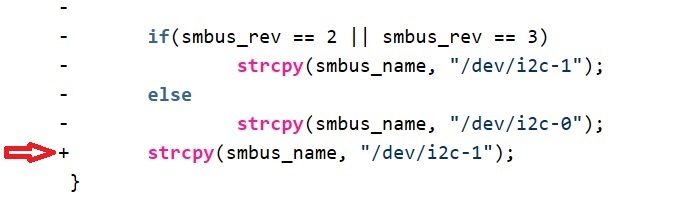
Xi2c9 on ARTIK 1020 does not support the SMBus Quick Command, so the i2cdetect utility will generate an error message for that bus.
i2cset – i2cget
i2cset and i2cget are small helper programs to set/get values of registers visible on the I2C bus. Specify one of the valid bus numbers with the command.
For example, the following command reads the byte value from the PMIC (s2mps14) register of ARTIK 520 at address 0x66 on I2C bus 0.
1 2 3 4 5 6 7 8 9 10 | # i2cget -f -y 0 0x66 0x0 0x00 # i2cget -f -y 0 0x66 0x1 0x03 # i2cget -f -y 0 0x66 0x2 0x11 # i2cget -f -y 0 0x66 0x3 0x00 # i2cget -f -y 0 0x66 0x4 0xff |
For the ARTIK 530 and 710, examples for addressing the sensors over I2C can be found here.
I2C using Python
You can also use Python scripts to access I2C interfaces through the SMBus module after installing the following packages:
apt install python-dev

apt install libffi-dev

apt install python-pip

pip install setuptools

pip install smbus-cffi
dnf install python-devel

dnf install redhat-rpm-config

dnf install libffi-devel

pip install smbus-cffi
Example 1. Enter ls -al /sys/class/i2c-dev/ to list the I2C adapters. If you see symlinks, go to the linked directory for easier viewing.
..

lrwxrwxrwx  1 root root 0 Sep 26 15:36 i2c-1 -> ../../devices/platform/c0000000.soc/c00a5000.i2c/i2c-1/i2c-dev/i2c-1
..
cd /sys/devices/platform
ls
Fixed MDIO bus.0    f0000000.0xf0000000  nexell-pcm    sd8x-rfkill
alarmtimer          gpio_keys            nx-devfreq    snd-soc-dummy
artik_s3t9mf        i2c@10               nx-v4l2       sound
artik_zb_power      i2c@4                panel-simple  spdif-out
c0000000.soc        i2c@5                power         thermal
c0010000.oscillator i2c@6                psci          uevent
c00e0000.busqos     i2c@7                pwm-backlight
camerasensor0       i2c@8                reg-dummy
cpu                 i2c@9                regulatory.0
In this example, you can see that you'll have access to I2C buses numbered 4 to 10.
You'll be using the SMBus module API to communicate with your device. Replace the 7 in SMBus(7) with your bus of interest, and replace the address 0x1d with the one you would like to read. Then save the code and run it (python i2c.py for example).
1 2 3 4 5 6 7 8 9 10 11 12 13 14 15 16 | import smbus
import time
bus = smbus.SMBus(7)
address = 0x1d
def status():
status1 = bus.read_byte_data(address, 1)
print(status1)
status2 = bus.read_byte_data(address, 2)
print(status2)
return
while True:
status()
time.sleep(1)
|
Example 2. If you have an ARTIK Sensor Board attached to your ARTIK 530 or 710, you also have access to bus 1. You could use a Python program to read the barometric pressure as shown in that article, for example.
Here we'll get you started. The bus is 1, the address is 0x5d. Reading the identification register at 0xf should return 189 (0xBD). For the rest, we're following the same sequence as shown in the tutorial to reset the device, write it to trigger, and then read back the results.
1 2 3 4 5 6 7 8 9 10 11 12 13 14 15 16 17 18 19 20 | import smbus
import time
bus = smbus.SMBus(1)
address = 0x5d
bus.write_byte_data(address, 0x21, 0xc4)
id1 = bus.read_byte_data(address, 0xf)
print(id1)
def status():
bus.write_byte_data(address, 0x20, 0x90)
preshigh = bus.read_byte_data(address,0x2a)
presmid = bus.read_byte_data(address,0x29)
preslow = bus.read_byte_data(address,0x28)
print(preshigh,presmid,preslow)
return
while True:
status()
time.sleep(1)
|
We'll leave it to you to write code to convert the three bytes to a final value in either hPa or inches of mercury.
I2C using Python with GrovePi+ Shield
If you are using an ARTIK "Eagleye" board with a Grove Pi+ shield kit as in the Face Detection article, you need to install I2C drivers.
-
Install these packages.
apt-get install g++ libi2c-dev -
Modify the source code /root/GrovePi/Software/Cpp/grovepi.cpp and add one line as shown.
-
Every time you reset the board, run the following two commands. Put them in a bash file to make it automatic.
1 2 | mkdir /sys/kernel/config/device-tree/overlays/i2c cat /boot/overlays/s5p4418-artik533-compy-i2c1.dtbo > /sys/kernel/config/device-tree/overlays/i2c/dtbo |
PWM Interface
ARTIK 520 and 1020 modules support two active-high PWM signal pins PWM0 and PWM1 (software-controlled as pwm0 and pwm1), and ARTIK 530/710 modules support signal pin PWM0 (software-controlled as pwm2), to generate periodic waveforms.
Mapping on ARTIK 520 and 1020
The default PWM mapping to pins differs between ARTIK 520 and ARTIK 1020. For convenience, the ARTIK 520 PWM output pins are reassigned in the Arduino IDE to make them match the ARTIK 1020. Some explanation may help clarify things.
Native Development Environment
The following table shows the default mapping of the PWM signals to the pins. The mappings apply when you are using Python or gcc, for example, to compile your code. They correspond to the sysfs pwm0 or pwm1 keywords as you would expect. It is possible to remap the assignments through kernel code, a topic not covered here.
| Header Pin artik 520 and 1020 |
Native Mapping ARTIK 520 rev 0.5 board |
Native Mapping ARTIK 1020 board* |
|---|---|---|
| J26[5] | PWM1 | PWM0 |
| J26[6] | PWM0 | PWM1 |
*Also on older ARTIK 520 rev 3.x boards
Arduino Integrated Development Environment
The libArduino board manager remaps the PWM signals to the appropriate location on connector J26 for Arduino shields. The "v0.5" selection swaps J26[5] and [6]. The remapping applies only to Arduino sketches, not to native or sysfs environments.

Open "Board Manager" and install the latest "ARM Linux Boards" package to get this option (go here for detailed instructions). Using the feature, the following table shows the mapping of the PWM signals to the pins.
| Header Pin | Mapping with 'Samsung Artik 520 v0.5' selected from Arduino IDE | As accessed from sysfs |
|---|---|---|
| J26[5] | XPWMO0 | pwm1 |
| J26[6] | XPWMO1 | pwm0 |
As you can see, choosing this reassignment within the Arduino IDE does not affect sysfs assignments – they match the 'native' environment for that board revision.
You can prove this to yourself with the exercises below. Use the Arduino IDE example to make an LED connected to J25[5] (corresponding to Arduino PWM#0) pulse on and off. Then, try to stop it from the command line by using unexport. You will find that it is pwm1, not pwm0, that has been exported.
Duplication on headers
The PWM outputs are duplicated across two headers; J513[1] and [2] are wired on the board to J26[5] and [6].
-
J26[5] = J513[1]
-
J26[6] = J513[2]
We show this to note that the pin swap issue between Native and Arduino programming modes affects both header sets. The ARTIK 520 ver. 0.5 board image below is labeled to show this, although it does not match the board silkscreen.
ARTIK 520 rev 0.5 Board

PWM control through sysfs
You can use sysfs to control the PWM outputs, either by command line interaction or by writing appropriate code (similar to that described for GPIO pins). Here is the path information you will need to export control of these pins.
#define SYSFS_PWM_PATH "/sys/class/pwm/pwmchip0/"
When you program the PWM:
- Maximum limit for
periodandduty_cycleis 1,000,000,000 (expressed in ns) duty_cycleshould always be less than period.
Kernel-level control of the PWM pins is typically not necessary unless the period or duty cycle are being rapidly modulated.
Exercise – Command Line
The following exercise demonstrates use of a PWM pin, setting a fixed blink rate. Connect PWM pin:
- ARTIK 1020: J26[5], controlled as
pwm0 - ARTIK 530 or 710: PWM0 (as marked on board), controlled as
pwm2 - ARTIK 520: J26[6] (for ARTIK 5 rev 0.5 boards), controlled as
pwm0
to an LED as in the Blink an LED tutorial to see the effect of the commands.
- Export PWM0
echo 0 > /sys/class/pwm/pwmchip0/export
Apwm0subdirectory is created. (You would useecho 1to createpwm1, or for the ARTIK 530/710, useecho 2to createpwm2.) -
Set attributes
a) Set period (Unit: ns) to 1 sec
echo 1000000000 > /sys/class/pwm/pwmchip0/pwm0/period
b) Set duty_cycle (Unit: ns) to 500 msec
echo 500000000 > /sys/class/pwm/pwmchip0/pwm0/duty_cycle
c) Enable PWM0
echo 1 > /sys/class/pwm/pwmchip0/pwm0/enable
d) Disable PWM0
echo 0 > /sys/class/pwm/pwmchip0/pwm0/enable - Unexport PWM0
echo 0 > /sys/class/pwm/pwmchip0/unexport
ThePWM0subdirectory is removed. (Or useecho 1orecho 2as noted above.)
Exercise – Arduino IDE
The following exercise demonstrates use of a PWM pin, making the LED pulse slowly on and off. Connect the PWM0 pin to an LED as in the Blink an LED tutorial to see the effect of the commands. Make sure you have selected your board correctly as noted in Arduino Integrated Development Environment.
-
Copy the following code into a blank sketch in the Arduino IDE.
1
2
3
4
5
6
7
8
9
10
11
12
13
14
15
16
17
18
19
20
const int thisPin = 5; void setup() { } void loop() { // brighten the LED for (int brightness = 0; brightness < 255; brightness++) { analogWrite(thisPin, brightness); delay(2); } // fade the LED for (int brightness = 255; brightness >= 0; brightness--) { analogWrite(thisPin, brightness); delay(2); } // pause between runs delay(100); } -
Load the code to ARTIK to run it.
ADC Interface
The ADC pins are available on the external connector pins of each development board as shown. Click on the header links to see the header mappings.
| ADC Pin reference in arduino |
ARTIK 520 j24 header |
ARTIK 530/710 test header |
ARTIK 1020 j24 header |
|---|---|---|---|
| ADC0 | J24[0] | [39] | J24[0] |
| ADC1 | J24[1] | [41] | J24[1] |
| ADC2 | [43] | J24[2] | |
| ADC3 | [45] | J24[3] | |
| ADC4 | [47] | J24[4] | |
| ADC5 | [49] | J24[5] | |
| – | [*] |
*With the sysfs interface, you will see ADC6 and ADC7 mappings. These are not available for external use.
ADC readback through sysfs
You can use sysfs to read the ADC inputs, initially by command line interaction and eventually by writing appropriate C, Python, or Arduino IDE code as described in Blink an LED. Here is the path information you will need.
ARTIK 1020:
/sys/devices/12d10000.adc/iio:device0/
ARTIK 530/710:
/sys/devices/platform/c0000000.soc/c0053000.adc/iio:device0/
ARTIK 520:
/sys/devices/126c0000.adc/iio:device0/
The following command line examples demonstrate how to read the current value of ADC pins 0 and 2, using different ARTIK boards as examples. In your application, substitute the path information for ARTIK module as needed.
-
Read a raw voltage from ADC0 of ARTIK 520
1
cat /sys/devices/126c0000.adc/iio:device0/in_voltage0_raw
-
Read a raw voltage from ADC2 of ARTIK 530 or 710
1
cat /sys/devices/platform/c0000000.soc/c0053000.adc/iio:device0/in_voltage2_raw
in_voltage0_raw returns a raw (unscaled) measurement value. To convert it to a voltage measurement, the equation :
v = in_voltageX_raw * 0.439453125 mV
is valid for the ARTIK module. Multiply v by 2 for the ARTIK development board, as it uses resistors to divide the input voltage by 2.
Kernel-level monitoring of the ADC pins is also possible, but may not provide a significant advantage over using the standard Linux routines.
C code to read the ADC port is provided below, using ARTIK 1020 mapping for this example.
1 2 3 4 5 6 7 8 9 10 11 12 13 14 15 16 17 18 19 20 | int analogRead(int pin) { FILE * fd; char fName[64]; char val[8]; // open value file sprintf(fName, "/sys/devices/12d10000.adc/iio:device0/in_voltage%d_raw", pin); if((fd = fopen(fName, "r")) == NULL) { printf("Error: can't open analog voltage value\n"); return 0; } fgets(val, 8, fd); fclose(fd); return atoi(val); } |
Exercise: Read Temperature Data
Use a TMP36 sensor to return a voltage proportional to temperature. Connect its middle pin to pin A0, pin 1 to +5V, and pin 3 to GND as shown in this figure for the TO-92 case version from the Analog Devices TMP36 data sheet.

Implement the following code to collect temperature sensor data every second using analogRead(), whose function code is shown above along with the formula for converting the analog sensor output to a voltage value.
1 2 3 4 5 6 7 8 9 10 11 12 13 14 15 16 17 18 19 20 21 | int inputPin = 0; int currentRun = 0; const int MAX_RUNS = 10; int main(void) { while(currentRun < MAX_RUNS){ int sensorVal = analogRead(inputPin); printf("current sensor is %f\n", sensorVal); /* convert sensor data to temperature here */ currentRun++; sleep(1); } } |